
This is preliminary information on a new product now in development or undergoing evaluation. Details are subject to change without notice.
16 Septembre 2002 Revision 1.1 1/62
AN1290
Application Note
How to Use the TDA911X and Improve Performances
®
TDA911x Deflection Processors at a Glance
The TDA911x is a family of deflection processors for multisync monitors, incorporating horizontal
and vertical processing, geometry correction, dynamic corrections (focus and/or brightness etc.),
DC/DC conversion and various safety and auxiliary functions. They are entirely controlled through
an I²C interface.
The TDA9112 was designed as an upgrade of the TDA9109/9111, using the same 32-pin shrink
DIP package. The pin-out remains nearly the same in order to simplify new layouts; however some
minor changes were necessary, mainly to pack more functions inside. Those already familiar with
TDA9109/9111 will recognize all the functions and operation styles they are accustomed to use.
For low- and medium-range applications where certain sophisticated features are not required,
several different economical versions of the TDA9112 are available: TDA9113, TDA9115 and
TDA9116. Table 1 summarizes their respective features. All versions are pin- and software-
compatible, with minor exceptions
1
.
Recently, the most complete version of the TDA9112 has been upgraded into the higher
performance TDA9112A. Improvements concern mainly geometry and focus corrections, but also
jitter behavior, B+ function, safety and I²C control. The design guidelines provide that the
TDA9112A should operate at once when fitted in the place of an existing TDA9112 (even if the
ideal I²C register settings may differ slightly).
Section 2: Special Features of the TDA9112A summarizes the improvements incorporated in
TDA9112A. For a detailed description of each, please refer to the relevant chapters.
1. Hard-wired H Moire function of the TDA9115/9116 replaces the Focus/Brightness functions.
Obsolete Product(s) - Obsolete Product(s)

Obsolete Product(s) - Obsolete Product(s)
AN1290
2/62 STMicroelectronics Confidential
Table of Contents
Chapter 1 Main Characteristics of the TDA9112 Deflection Processor Family . . . . . . . . .5
Chapter 2 Special Features of the TDA9112A . . . . . . . . . . . . . . . . . . . . . . . . . . . . . . . . . . . .7
Chapter 3 TDA9112 Family Pin Review . . . . . . . . . . . . . . . . . . . . . . . . . . . . . . . . . . . . . . . . .9
Chapter 4 Horizontal Section . . . . . . . . . . . . . . . . . . . . . . . . . . . . . . . . . . . . . . . . . . . . . . . .11
4.1 Theory of Operation ...........................................................................................................11
4.1.1 Horizontal Section Structure ..............................................................................................................11
4.1.2 Digital Sync Detection ........................................................................................................................12
4.1.3 Composite Sync .................................................................................................................................12
4.1.4 Voltage-controlled Oscillator ..............................................................................................................12
4.1.5 PLL1 ..................................................................................................................................................13
4.1.6 Free-running Frequency and Range ..................................................................................................13
4.1.7 Frequency Precision ..........................................................................................................................14
4.1.8 PLL1 Inhibition ...................................................................................................................................15
4.1.9 Frequency Change Speed Limitation .................................................................................................16
4.1.10 PLL2, Duty Factor, ON/OFF ...............................................................................................................16
4.1.11 Soft-start ............................................................................................................................................17
4.1.12 Output Stage ......................................................................................................................................17
4.1.13 X-ray Protection .................................................................................................................................17
4.1.14 Lock-Unlock Detection .......................................................................................................................17
4.1.15 H Moire Cancellation .........................................................................................................................18
4.2 Application Hints ................................................................................................................19
4.2.1 Minimizing Jitter .................................................................................................................................19
4.2.2 Output Stage ......................................................................................................................................20
4.2.3 Enlarging the Frequency Range ........................................................................................................21
4.2.4 X-Ray Protection ................................................................................................................................22
Chapter 5 Vertical Section . . . . . . . . . . . . . . . . . . . . . . . . . . . . . . . . . . . . . . . . . . . . . . . . . .23
5.1 Theory of Operation ...........................................................................................................23
5.1.1 Structure of V Section ........................................................................................................................23
5.1.2 Ramp Generator and AGC Loop .......................................................................................................23
5.1.3 Frequency Range and Precision ........................................................................................................24
5.1.4 Sync Detection ...................................................................................................................................25
5.1.5 AGC Loop Stability .............................................................................................................................26
5.1.6 S and C Correction (TDA9112 to TDA9116) ......................................................................................26
5.1.7 Output Stage and Vertical Shift ..........................................................................................................28
5.1.8 Vertical Signal Management in the TDA9112A ..................................................................................29
5.1.9 ON/OFF Function ..............................................................................................................................30
5.1.10 V Lock/Unlock ....................................................................................................................................30
5.1.11 V Moire ..............................................................................................................................................31
5.1.12 Vertical Breathing Function (EHT Compensation) .............................................................................31
5.1.13 Implementing the Breathing Function ................................................................................................31

Obsolete Product(s) - Obsolete Product(s)
STMicroelectronics Confidential 3/62
AN1290
5.1.14 Breathing Functions in the TDA9112A ...............................................................................................33
5.2 Application Hints ................................................................................................................33
5.2.1 Coupling to Booster ...........................................................................................................................33
5.2.2 Ripple Rejection .................................................................................................................................34
5.2.3 Vertical Vibration ................................................................................................................................35
5.2.4 Leakage on Cs ...................................................................................................................................36
Chapter 6 Geometry and Focus Control Section . . . . . . . . . . . . . . . . . . . . . . . . . . . . . . . .37
6.1 Theory of Operation ...........................................................................................................37
6.1.1 Geometry Corrections through E/W (PCC) Output ............................................................................37
6.1.2 Tracking with Horizontal Size .............................................................................................................39
6.1.3 Tracking with Horizontal Frequency ...................................................................................................39
6.1.4 Geometry Corrections through HPhase Control ................................................................................39
6.1.5 Tracking with Vertical .........................................................................................................................39
6.1.6 Dynamic Corrections .........................................................................................................................40
6.1.7 Horizontal Dynamic Focus/Brightness ...............................................................................................40
6.1.8 Vertical Dynamic Focus/Brightness ...................................................................................................41
6.1.9 Vertical Dynamic Focus .....................................................................................................................41
6.2 Application Hints ................................................................................................................42
6.2.1 E/W Output Stage ..............................................................................................................................42
Chapter 7 DC/DC Converter Section . . . . . . . . . . . . . . . . . . . . . . . . . . . . . . . . . . . . . . . . . .44
7.1 Structure of the DC/DC Converter and B+ Loop ................................................................44
7.1.1 Structure of the Converter Section ....................................................................................................44
7.1.2 External or Internal Sawtooth Configuration ......................................................................................44
7.1.3 B+ Output Polarity ..............................................................................................................................45
7.1.4 Soft-start ............................................................................................................................................45
7.1.5 Selecting the Trigger Timing ..............................................................................................................46
7.1.6 Structure of the Regulation Loop (Step-up, Current mode) ...............................................................46
7.1.7 Structure of the Regulation Loop (Step-down, Current Mode) ..........................................................47
7.1.8 Structure of the Regulation Loop (Step-down, Voltage mode) ...........................................................48
7.1.9 Structure of the DC/DC Converter (Open Loop) ................................................................................49
7.2 Application Hints ................................................................................................................50
7.2.1 Parasites induced by DC/DC Converter (Timing Selection) ...............................................................50
7.2.2 Frame-top Distortion related to Keystone Correction .........................................................................51
Chapter 8 Miscellaneous . . . . . . . . . . . . . . . . . . . . . . . . . . . . . . . . . . . . . . . . . . . . . . . . . . . .52
8.1 Summary of Safety Functions ............................................................................................52
8.2 Early V Blanking and Lock/Unlock .....................................................................................53
8.3 Application Hints ................................................................................................................53
8.3.1 Using Inhibition Properly ....................................................................................................................53
Chapter 9 I²C Control Section . . . . . . . . . . . . . . . . . . . . . . . . . . . . . . . . . . . . . . . . . . . . . . . .55
9.1 I²C Bus Reminder ...............................................................................................................55

Obsolete Product(s) - Obsolete Product(s)
AN1290
4/62 STMicroelectronics Confidential
9.2 TDA9112 Family as I²C Bus Device ...................................................................................55
9.3 Receiving Data ...................................................................................................................55
9.4 Sending Data .....................................................................................................................56
9.5 Register Organization ........................................................................................................56
9.6 Management of Status Register and Sync Priority ............................................................58
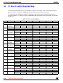
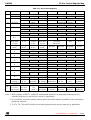
Chapter 10 I²C Bus Control Register Map . . . . . . . . . . . . . . . . . . . . . . . . . . . . . . . . . . . . . . .60

Obsolete Product(s) - Obsolete Product(s)
STMicroelectronics Confidential 5/62
AN1290 Main Characteristics of the TDA9112 Deflection Processor Family
1 Main Characteristics of the TDA9112 Deflection
Processor Family
Control
● Control of all functions and status reading through I²C interface (status reading is not available
with the TDA9115).
● I²C settings take effect during the Vertical Oscillator Retrace for an improved screen aspect.
These parameters can be sent at any moment.
Horizontal
● Dual PLL structure
● Maximum frequency of 150 kHz
● Self-adaptable frequency range from 1 to 4.5 or more
● Improved jitter control functions
● X-ray protection with digital filtering
● Lock/Unlock output; data also available on I²C bus (except for the TDA9115)
● ON/OFF Output function for Power Management
● I²C control of duty cycle, H-position and H-amplitude values with frequency tracking if required
● Smooth frequency transitions
● Internal soft-start
Vertical
● Constant amplitude, self-adaptive vertical ramp generator
● 50 to 185 Hz frequency range
● ON/OFF Output function for Power Management
● I²C control of V-amplitude, V-position, S- and C-correction amplitudes
● S-correction adapted to normal or super-flat tubes
● Lock/Unlock data by I²C (except for the TDA9115)
● Signal for early V Blanking.
East/West Pincushion Correction and Advanced Geometry Corrections
● Pincushion Parabola generator, with DC coupling possible for H-Size control
● I²C control of Pincushion, H-amplitude, Keystone and Corner corrections
● Corner correction, top and bottom independent, symmetric and asymmetric
— No symmetric corner correction for the TDA9115; no asymmetric corner correction for the
TDA9113, the TDA9115 and the TDA9116
● H and V compensations of EHV variations (breathing inputs)
● Auto-tracking of all the corrections above with H-frequency (if required) and H-amplitude
● I²C control of parallelogram and side-pin balance correction
● Auto-tracking of all geometry corrections with V-amplitude and V-position

Obsolete Product(s) - Obsolete Product(s)
Main Characteristics of the TDA9112 Deflection Processor Family AN1290
6/62 STMicroelectronics Confidential
Dynamic Correction
● Auto tracking with V-position and V-amplitude
● Composite Dynamic output (e.g. focus or brightness) providing:
— Horizontal Parabola with I²C control of amplitude and symmetry (except for the
TDA9115/9116)
— Vertical parabola with I²C control of amplitude (TDA9112 only).
● Extra dynamic output with programmable polarity (e.g. separate V focus)
DC/DC Converter
● Control section for DC/DC converter, based on UC 3842 architecture
● Programmable for step-up or step-down configurations
● In step-down mode, control of power P-MOS transistor without transformer, or N-MOS
transistor through transformer.
● Internal soft-start
● Can operate as open-loop converter.
Miscellaneous
● Accepts positive and negative H and V sync signals
● Accepts Composite sync signals with the automatic management of serration pulses
● Sync on Green is not extracted (this function is available in ST Video preamps)
● Vertical Moire compensation controlled by I²C programming
● Horizontal Moire compensation (I²C programming), may be optimized for combined or separate
structure (EHV/Scanning).
— TDA9112/9113/9116: self-contained
— TDA9115/9116: hardwired
● I²C bus can read Sync polarity and status, Lock/Unlock status and X-ray status (except the
TDA9115).
● I²C can reset X-ray status.
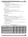
Table 1 summarizes the differences between the various family versions.
Table 1: Family Differences
Description 9112 - 9113 - 9115 - 9116 -
I²C Status reading (sync status, Lock/Unlock, X-ray) Yes Yes No Yes
Symmetrical Corner Correction Yes Yes No Yes
Asymmetric Corner Correction Yes No No No
Pin 11 function Comp DyCor Hor DyCor Moire Moire/DAC
DC/DC converter with internal sawtooth Yes No No No
I²C programmable DC/DC converter reference Yes Yes No Yes
Internal/Hardwired Moire Int Int Ext Int/Ext

Obsolete Product(s) - Obsolete Product(s)
STMicroelectronics Confidential 7/62
AN1290 Special Features of the TDA9112A
2 Special Features of the TDA9112A
The TDA9112A provides features and performances at least equal to those of the TDA9112, with
one exception: the DC/DC converter configuration using an internal oscillator has not been
continued because very few customers used it. Software compatibility is maintained.
The new or improved functions are listed below and details may be found in the relevant chapters.
The most important improvements concern geometry and focus correction.
Control
● 8-bit control of the H-size and H-position. Compatibility with the rest of the family is maintained
since only the LSB is affected.
● A dedicated bit enables the MCU to automatically detect whether the circuit present is the
TDA9112 or the TDA9112A.
Horizontal
● In PLL1, now there is a choice between 4 values of the charge-pump current, to better optimize
jitter in relation to the horizontal frequency.
● The indication of H-frequency Unlock can be made twice as fast as previously.
Vertical
● The block diagram of S and C linearity corrections has been modified to fit in the “tracking”
feature. As a result, it is possible to adjust amplitude or to switch between the VGA modes
without impairing linearity.
● The law of S correction has been modified, allowing perfect fitting to various types of tubes.
● Further to regular amplitude and centring settings (which maintain ideal linearity and
pincushion correction thanks to the “tracking” feature), the new prescale settings (without
tracking feature) provide better flexibility, for instance to adapt one chassis to various tubes.
● New EHT compensation has a two-quadrant sensitivity adjustment (i.e. you can choose the
compensation sign as well). This allows perfect compensation throughout the H-frequency
range.
East/West Pin Cushion Correction and Advanced Geometry Corrections
● Two new controls of E/W are provided, namely S and W control. Their action is symmetrical
versus center. They leave top, bottom and middle of the screen unaffected:
— S correction inflates the top 1/4 and deflates the bottom 3/4 or the opposite,
— W correction inflates top 1/4 and bottom 3/4, or deflates both.
These corrections may help prevent certain distortions related to the DC/DC converter.
● A control bit can disable the tracking of E/W corrections versus H-amplitude.
● New EHT compensation has a two-quadrant sensitivity adjustment, independent of the one for
the Vertical section.

Obsolete Product(s) - Obsolete Product(s)
Special Features of the TDA9112A AN1290
8/62 STMicroelectronics Confidential
Dynamic Correction (Focus/Brightness)
● The new composite H/V output can provide any signal polarity (concavity up or down; same
polarity for H and V).
● The signal at horizontal frequency, previously parabolic, may be set to any power index from 2
to 4. Indeed the useful range is from 2 to 2.5, to adapt to various tubes available on the market.
● Because the combination of high power index and phase setting may lead to high transients
during H flyback, means are provided to limit transients.
DC/DC Converter
As previously mentioned, the “Internal sawtooth” configuration is no longer available. Improvements
include:
● Choice of the maximum current threshold using pin 16 (Isense): previous 2V is convenient
when implementing a sawtooth oscillator, but the new value 1.2V (same as in UC 384x family)
is better adapted for Isense, as in current-mode step-up converters.
● A new control bit performs the ON/OFF function, independently of Horizontal and with soft-
start.
● In addition to the three possible phases for the DC/DC converter (HOut Up, HOut Down, after
HFlyback), a new option is: triggered with top of H sawtooth, with frequency divided by 2. It
may extend the range of step-up converters to higher frequencies. Nevertheless, careful
filtering and parasitic suppression will be necessary.
Miscellaneous
● B+ Safety: If the control bit is selected, the DC/DC converter will stop whenever HLock is lost.
Restart will take place in a soft way.
● Internal current sinks: E/W and Dynamic correction outputs (pins 11, 24 and 32) now have an
internal current sink which in most cases makes an external resistor unnecessary.

Obsolete Product(s) - Obsolete Product(s)
STMicroelectronics Confidential 9/62
AN1290 TDA911x Family Pin Review
3 TDA911x Family Pin Review
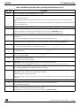
The main features of the TDA9112, TDA9113, TDA9115 and TDA9116 are described in Table 2.
The additional features for the TDA9112A are given in Section 2: Special Features of the
TDA9112A.
Table 2: TDA911x Pin Descriptions (Sheet 1 of 2)
Pin No. Pin Description
1 Receives Horizontal or Composite sync signals (TTL compatible, threshold approximately 1.4V, any polarity).
2 Receives separate V sync signals (same level as pin 1, any polarity).
Warning! The functionality of pins 1 and 2 may be affected by I²C.
3 Provides an early V blanking signal (amplitude 1V, High = Blank) to be ORed with V retrace ; combined with an H
Lock/Unlock signal (amplitude 5V, High = Unlocked).
Warning! Blanking and H Lock/Unlock functions are programmable through I²C.
4 Should be filtered to HGND, it improves H Jitter by filtering the H oscillator peak level.
5 (PLL2 filter) should be filtered to HGND (typical value 22nF), it improves jitter by filtering the level at which the
scanning is triggered.
6 The oscillator capacitor Co (typically 820pF) is connected between Pin 6 and HGND. A sawtooth at H frequency will
appear on this pin.
7 HGND; to be connected to General Ground pin 27 and to the components of H section only.
8 The oscillator resistor Ro (typically 5.2kΩ) is connected between Pin 8 and HGND. Co·Ro sets the free-running
frequency as Fo = 0.1215 / (Co·Ro). Voltage on pin 8 is always the same as on Pin 9.
9 The PLL1 loop filter is connected between pin 9 and HGND: 10nF to HGND, and in parallel: 1.8kΩ in series to 4.7µF
electrolytic. The electrolytic sets the speed of H-frequency change when sending a new video mode; the other
components are critical for H jitter characteristics. Voltage on pin 9 is proportional to H Oscillator frequency.
10 Should be filtered to HGND, it improves H jitter by filtering the DC level for H position. Capacitor on pin 10 also sets
the time constant for soft-start.
11 Output pin for composite dynamic H/V Focus (or Brightness). The waveform on this pin is the sum of two parabolas,
one at horizontal frequency, one at vertical frequency. The internal structure is NPN emitter-follower; a pull-down
resistor (10kΩ) is recommended.
The TDA9113 has an H-frequency parabola only.
On the TDA9115 and the TDA9116, dynamic focus is absent, H-Moire compensation is available in the place. To use
it, connect pin 11 to HGND through a resistor divider with ratio of 1000 to 2000, connect the low side of PLL2
capacitor to the middle point (rather than to HGND).
Warning! In the TDA9116, H Moire is I²C-programmable as either external (available on pin 11) or internal; in latter
case, pin 11 is a DAC with a voltage range between 0 and 5V.
12 H Flyback input, a voltage comparator (the base of a NPN transistor with emitter grounded). It should be connected to
a positive H flyback pulse; a resistor connected in series is necessary to limit the input current to less than 5 mA while
the pulse is positive.
13 Reference voltage, 8V nominal, to be filtered versus HGND. Since there is no reference voltage dedicated to the
Vertical section, pin 13 should also be used for biasing the non-inverting input of vertical booster through a suitable
resistor bridge.
14 Output of the op-amp that amplifies the error signal of the DC/DC converter feedback loop. Its voltage sets the current
level (represented by voltage on pin 16) at which the power MOS transistor will switch OFF.
15 Inverting input of the same op-amp.The feedback elements (typically 1MΩ parallel to 10nF) should be connected
between pins 14 and 15. The op-amp non-inverting input is not available; it is internally biased by a 4.8V reference
voltage, adjustable through I²C (except the TDA9115).

Obsolete Product(s) - Obsolete Product(s)
TDA911x Family Pin Review AN1290
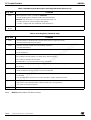
10/62 STMicroelectronics Confidential
16 When the DC/DC converter is used in the External sawtooth configuration, Pin 16 should receive a sawtooth (less
than 2V peak), either representative of the current in the switch (current mode) or provided by an R/C oscillator (open
loop). In both cases, the power MOS transistor is switched OFF when pin 16 voltage exceeds one-third of the voltage
on pin 14. Biasing Pin 16 with more than 6V will set the so-called “internal sawtooth”, in voltage mode configuration
(TDA9112 only).
17 & 18 High-impedance inputs which control H and V amplitude respectively. Each one should receive an image of the EHT
(for instance, a fraction of the Automatic Beam Limiter voltage) for size compensation versus EHT variations. Both
have the same active range: 1 to 8V, and sign: amplitude increases when pin voltage increases. The gains of the two
channels have to be separately set to the correct values by external resistive dividers.
19 Presents a DC level equal to Vertical sawtooth negative peak, it should be filtered to VGND to improve vertical jitter.
20 The capacitor on pin 20 stores the AGC value to maintain the constant Vertical Sawtooth amplitude regardless of the
frequency. It should be a 0.47µF non-electrolytic capacitor.
21 Vertical ground. In addition to the main GND on pin 27, it should be only connected to Vertical section components.
22 A 0.15µF film capacitor should be connected between Pin 22 and VGND to obtain the Vertical Sawtooth with constant
amplitude (between 2 and 5V).
23 The same sawtooth is available on pin 23, buffered and with adjustable amplitude and offset for the control of vertical
size and position. The middle value of this signal is (3.5/8) of the reference voltage (pin 13). An equal voltage should
be derived from pin 13 through a resistive divider, to bias the Vertical booster positive input.
24 Provides the complete waveform to control Horizontal amplitude, including DC (for H Size, with EHV compensation),
Pincushion, Keystone and symmetric Corner. It has the structure of an Emitter follower; a pull-down resistor (10kΩ) is
necessary. Voltage range is 2 V to 8.5 V. The TDA9115 does not have corner correction.
25 High-impedance comparator input for X-ray detection, with 8V threshold. It should be filtered to GND (VGND is
recommended).
26 HOut: open-collector NPN with more than 30mA capability. The NPN is switched OFF (pin 26 High) when the
scanning transistor is to be switched OFF (“Reverse control”). An external pull-up resistor connected to pin 29 is
necessary. Direct control of a bipolar NPN driver is possible.
27 General GND. The general GND track should enter the IC area by this pin, then be connected only to the special H
and V ground tracks.
28 BOut: open-collector NPN, with more than 10mA capability. An external pull-up resistor connected to pin 29 will be
necessary to make the power switch conductive.
Warning! The polarity should be selected by I²C. By default: High level (NPN OFF) is meant to make the power switch
conductive (adapted for N-type power switches).
29 General supply (10.8 V to 13.2 V, 70 mA). It should be filtered to pin 27.
30 & 31 SCL and SDA for the high-speed I²C bus. Threshold voltage is 2.2V typically.
32 Extra V Focus output, to allow separate H Focus and V Focus channels. It provides a parabola at Vertical frequency.
It presents the structure of an emitter follower and requires a 10 kΩ pull-down resistor to GND. Quiescent voltage is
4V.
Warning! The signal polarity may be selected through I²C (Default is: Downwards Concavity ∩).
Table 2: TDA911x Pin Descriptions (Sheet 2 of 2)
Pin No. Pin Description

Obsolete Product(s) - Obsolete Product(s)
STMicroelectronics Confidential 11/62
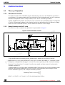
AN1290 Horizontal Section
4 Horizontal Section
4.1 Theory of Operation
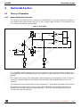
4.1.1 Horizontal Section Structure
The TDA9112 horizontal section is similar to the TDA9109/9111. It includes a sawtooth oscillator, a
sync detector, two phase-locked loops (PLLs) and an output stage. Moreover, X-ray protection and
PLL1 lock/unlock detection are provided.
PLL1 locks the oscillator frequency to the HSync frequency, then adjusts its phase, until the sync
pulse coincides with an adjustable level on the sawtooth. Changing the level is used to adjust the H-
position.
PLL2 adjusts the phase of the output stage (compensating for the storage time of the H scanning
transistor), until the middle of the H flyback pulse coincides with a predetermined level on the
sawtooth.
The horizontal phase and duty factor may be adjusted by I²C programming (Registers 00h and 01h).
All voltage values meaningful for the H section (like comparator and oscillator thresholds) are
derived from a common reference voltage (between 7.4V to 8.6V with 8V typical) and keep a
constant ratio with this reference.
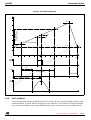
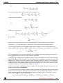
Figure 1: H Oscillator
8 6
V9
0.5 x I8
6.4V
1.6V
R0
C0
S
R
4 x I8
I8

Obsolete Product(s) - Obsolete Product(s)
Horizontal Section AN1290
12/62 STMicroelectronics Confidential
4.1.2 Digital Sync Detection
The H/HV sync pulse is detected on pin 1 by a comparator with hysteresis, compatible with the
standard TTL. It is intended for digital sync only (separate or composite). The IC synchronizes on
the pulse front edge. A pull-down resistor (200 k
Ω) is included.
Sync polarity recognition is performed as follows: The comparator output controls the charge or
discharge of an internal 50pF capacitor with ±0.1µA current. Depending on the polarity of the sync
signal, the capacitor voltage will either drift towards the ground or the 8V supply. A comparison of
capacitor voltage with a 4V threshold indicates the sync polarity. The recognition delay is
approximately 2ms (typical) with a minimum value of 0.75 ms. This way, in the event of a Composite
sync signal, vertical sync pulses up to 0.75ms will not be unduly interpreted as a change in HSync
polarity.
Þ Serration pulses: When they are missing, the inhibition of PLL1 during Vertical sync pulse
(described later) prevents any disturbance of the Horizontal oscillator. For this purpose, the
composite V pulse must be recognized within one horizontal half-period (see Section
4.1.3: Composite Sync).
4.1.3 Composite Sync
In order to extract the VSync pulse from the composite signal, the duration of each sync pulse is
compared with the horizontal period. As soon as the duration of a pulse exceeds 21% (minimum) of
the horizontal period (30% typical), this pulse is recognized as a VSync pulse.
The VSync duration measurement uses an internal capacitor and a current source that keeps a
constant ratio with Horizontal oscillator current source. Consequently, the system will work as
indicated only if the recommended value of 820 pF for oscillator capacitor Co is applied.
Otherwise for instance, when using a higher value, at the same frequency, all charge currents will be
higher and therefore the recognition delay will decrease possibly to less than 21% of the horizontal
period. This would lead to the incorrect detection of the Vertical Sync signal.
See Section 9: I²C Control Section for more information about sync management through I²C
programming.
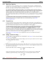
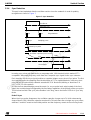
4.1.4 Voltage-controlled Oscillator
The H oscillator is similar to the one in the TDA9109/9111. See Figure 1 for the schematic diagram
and Figure 2 for waveforms.
A voltage-follower stage imposes the same voltage on pin 8 as on pin 9, which is the PLL1 output.
The current in pin 8 is then fixed to:
Current mirroring provides two current sources, with values of 0.5 x I
8
(“source”) and 4 x I
8
(“sink”).
Two comparators with thresholds of respectively 1.6V and 6.4V control a toggle that switches ON or
OFF the 4 x I
8
current source.
Supposing this latter source is initially OFF, capacitor C
0
will charge at a rate:
until the 6.4V threshold is reached. At that moment, the 4 x I
8
current source is switched ON,
establishing a global discharge current equal to 3.5 x I
8
. Discharge will continue at a rate:
I
8
V
8
R
0
-------=
dV
dt
-------
0.5xI
8
C
0
-----------------=
dV
dt
-------
3.5xI
8
C
0
-----------------=

Obsolete Product(s) - Obsolete Product(s)
STMicroelectronics Confidential 13/62
AN1290 Horizontal Section
until the 1.6V threshold is reached; then a new charge phase starts. As a result, the voltage on pin
6 will be a sawtooth with a (6.4-1.6)V amplitude and a period of:
Replacing I
8
by its value and taking the reverse, one obtains the theoretical formula:
If I
8
exceeds 1.5 mA, the oscillator components will not work in the optimal conditions; moreover, if
at the same time V
8
is higher than 6.2 V, there is a risk of saturation of internal circuitry. These two
reasons combined led to recommend R
0
>4.2kΩ.
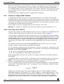
Note: All details relative to the oscillator waveform are represented in Figure 2 with: Period = 12 µs,
Flyback duration = 3.2 µs, Duty factor = 50%, Sync pulse duration = 1 µs, Storage time = 2 µs.
4.1.5 PLL1
The aim of PLL1 is to control the oscillator's frequency and phase, until the front edge of the H sync
pulse just coincides with a determined (and adjustable) voltage (V
φ
) on the sawtooth.
Two current generators (one “source” and one “sink”) are connected to the PLL1 output (pin 9). This
pin is connected to an external low-pass filter, it controls pin 8 voltage through a voltage follower.
● If the front edge of the HSync pulse arrives before the V
φ
point on sawtooth, the “source”
current is activated in the interval: this will increase the voltage and the oscillation frequency.
● If the V
φ
point on sawtooth arrives before the HSync pulse front edge, the “sink” current is
activated in the interval, this will decrease the oscillation frequency;
● when PLL1 is locked, there is a very narrow “source” current pulse just before the V
φ
point and
a very narrow “sink” pulse just after; therefore the voltage on pin 9 remains stable.
V
φ
may be adjusted by ±0.6V around the average value of 3.4V, through I²C programming (Register
01), allowing a control of the horizontal phase, up to ±10% of a period. For an optimum jitter, pin 10
should be filtered to GND (no limit on the capacitor value. It also sets the soft-start time constant).
The PLL1 capture range is large enough to synchronize with all incoming sync frequencies.
Normally, both “sink” and “source” currents should be set to 1mA, and the recommended
components in PLL filter are optimized accordingly. Nevertheless, the current value may be
switched to 0.3 mA by I²C programming (Sad16h/d3:2). Jitter may be improved by switching to
0.3 mA at low frequencies and to 1 mA at high frequencies. The default value is 0.3 mA.
In the TDA9112A there are four values for the current that can be selected by I²C programming
(Sad16h/d3:2).
4.1.6 Free-running Frequency and Range
When HSync pulses are absent or at low frequency, the PLL1 output will clamp to 1.33 V, which
corresponds to the free-run frequency (f
0
). From the formula for frequency, we get:
∆T
h
C
0
x ∆V
1
0.5xI
8
-----------------
1
3.5xI
8
-----------------+
èø
æö
èø
æö
with∆V6.41.6
– 4.8===
f
h
V
8
2.286x R
0
xC
0
x∆V()()
-----------------------------------------------------------
V
8
10.97x R
0
xC
0
()
-------------------------------------------==
f
0
1.33
10.97x R
0
xC
0
()
-------------------------------------------
0.1215
R
0
xC
0
-------------------==

Obsolete Product(s) - Obsolete Product(s)
Horizontal Section AN1290
14/62 STMicroelectronics Confidential
When HSync pulses are received, the voltage on pin 9 will increase until the local oscillator matches
the incoming frequency. Since the range for pin 9 voltage is between 1.3V and 6.2V, the relative
capture frequency range (ratio of maximum to minimum frequency) is:
4.1.7 Frequency Precision
All the terms in the f
0
equation have a spread. Both voltages are derived from the same reference,
their ratio will remain quite accurate. In regards to the other variables, we have to consider a
tolerance of ±1% for R, ±5 or 10% for C and ±6% for the numerical factor which incorporates a
current ratio.
Consequently the free-running frequency can vary from ±12 or 17% of the designed value, using
safety margins can reduce the usable relative frequency range by 2 x 12% or 2 x 17%; or ±9% if you
can afford a ±2% capacitor.
An other consequence of the free-running frequency spread is to make the design of a B+ converter
more difficult, because in free-running mode, the B+ converter may have to follow the oscillator
frequency down to low values. (This may be avoided if fake HSync pulses are sent by the MCU at a
convenient frequency, as soon as there is no sync coming through the input plugs.)
6.2
1.3
--------4.77=

Obsolete Product(s) - Obsolete Product(s)
STMicroelectronics Confidential 15/62
AN1290 Horizontal Section
4.1.8 PLL1 Inhibition
The PLL1 operation remains undisturbed if one (and only one) sync pulse front edge arrives in each
horizontal period, in phase with the V
φ
point on each sawtooth. In the event of a composite digital
sync pulse, this condition is no longer fulfilled during Vsync, when there are no serration pulses.
Figure 2: H Oscillator Waveform
6.4V
1.6V
V
0
5
5
Duty factor
setting voltage
10 12µs
V
Sync
pulse
V26
PLL2 Threshold
Range for PLL2
Forced OFF
Forced ON
Fly
back
t
st
φ
4V

Obsolete Product(s) - Obsolete Product(s)
Horizontal Section AN1290
16/62 STMicroelectronics Confidential
When PLL1 endures this severe disturbance, it requires some time to recover the proper phase. As
this could entail a visible distortion on top of the screen, the TDA9112 has been provided with a
PLL1 inhibition feature: the two current sources of PLL1 will be turned OFF during the Vsync pulse
and 2 complete lines later. Internal inhibition is activated only by the Vsync pulse extracted from
composite sync.
This features may be disabled through I²C programming (Sad16h/d1).
4.1.9 Frequency Change Speed Limitation
It is well-known that when receiving a new horizontal frequency, PLL1 should not synchronize
immediately with the new frequency, especially when it is lower than the former one. Otherwise the
horizontal scanning transistor would conduct for a longer period of time, while the value of B+ would
not have time to decrease to its newly assigned lower value. This would lead to excessive current
and voltage and possibly destroy the transistor.
In the TDA9112, the PLL1 changing speed has been limited to a safe value.
Warning! This limitation is ineffective when imposing a frequency jump by switching Ro or Co.
4.1.10 PLL2, Duty Factor, ON/OFF
Supposing the oscillator is locked to the Hsync pulse, then PLL2 controls the H scanning transistor
so that the flyback takes place at a definite point on the sawtooth. (Refer to Figure 2.)
For this purpose, a positive flyback signal must be sent to pin 12, which is connected to a voltage
comparator with a threshold of one V
BE
, and to the Ground through a 20kΩ (typical) resistor. Among
other possibilities, pin 12 may be connected to a secondary of the scanning transformer through a
current-limiting resistor. In order to allow lower values of the limiting resistor, and therefore faster
transmission of the flyback data, the maximum input current into this pin has been increased to
5mA.
The reference point for PLL2 is the middle of the flyback pulse (as seen on pin 12). PLL2 will
manage to make it coincide with the 4V point on the sawtooth.
PLL2 is a classical charge pump PLL. Its output (pin 5) must be connected to a capacitor as a low-
pass filter. For the entire flyback pulse duration, one of the two 0.15-mA internal current generators
connected to pin 5 will be activated:
● the source current, when the ramp voltage is lower than 4 V,
● the sink current, when the ramp voltage is higher than 4 V.
With the flyback pulse centred on the 4V point, the capacitor will receive a null global charge for
each period.
The capacitor value is not critical (22nF for good jitter). With a low capacitor value, PLL2 will more
rapidly recover of any change in the H transistor storage time caused by a black/white video
transition. This will minimize the corresponding distortion of vertical lines.
The Pin 5 voltage directly controls which point on the sawtooth will trigger the scanning transistor
switching OFF. The possible range for pin 5 is between 1.6V and 4V, allowing a transistor storage
time between 0 and:
Similarly, the scanning transistor ON state is triggered when the oscillator sawtooth reaches a
determined voltage; the offset between OFF and ON voltages is constant (adjustable by I²C). As a
result, the TDA9112 will maintain constant duty factor, regardless of PLL2 voltage variations. The
typical Duty factor range is between 30% and 65% and is selected through I²C programming
(Register 00). This is the OFF duty factor, i.e. the ratio of the OFF drive time to the total period.
0.438x T
h
t
flyback
2
----------------------
–
èø
æö
èø
æö

Obsolete Product(s) - Obsolete Product(s)
STMicroelectronics Confidential 17/62
AN1290 Horizontal Section
Hex code 00 corresponds to a 65% duty factor. This is the default value at start-up, in order to
minimize the stress on the scanning transistor.
4.1.11 Soft-start
The TDA9112 is equipped with a self-contained soft-start. When switching ON, HOut will remain
inhibited until the supply voltage ramps up to more than 8.5V. Afterwards, the initial duty factor will
progressively decrease from 85% to 65% (the scanning transistor will be controlled OFF for 65% of
the period), then to the value that has been set through I²C programming. The same events will take
place in the reverse order when the supply ramps down through a 6.5V threshold (thresholds for
TDA9112A: 8.0V and 6.8V).
The time constant that controls the soft-start is the charge rate of H-position capacitor on pin 10.
The soft-start is effective when switching ON and when resetting the HOut inhibition. It also controls
the duty factor of the DC/DC converter (except in the so-called “internal sawtooth, voltage mode
configuration”). For more information, refer to Section 7: DC/DC Converter Section.
4.1.12 Output Stage
The drive signal for the H scanning transistor is available on pin 26, which is connected to the
collector of the output NPN transistor. The transistor is conductive (pin 26 LOW) when the H
scanning transistor is to be ON and vice-versa. Pin 26 should be connected to the supply through a
pull-up resistor. Of course, some kind of driver stage is mandatory to control the scanning transistor
base.
The saturation voltage on pin 26 (less than 0.4V for 30mA) is low enough to allow direct control of a
bipolar driver. Nevertheless and for other reasons we recommend keeping an AC coupling between
pin 26 and the driver. For more information, refer to Section 4.2.2: Output Stage.
The output transistor is forced ON during the negative slope part of the sawtooth. It is forced OFF
during flyback (as seen on pin 12), and this safety function has the priority over any other control.
The goal is to prevent the scanning transistor from turning ON again, while it still sustains the high
flyback voltage.
4.1.13 X-ray Protection
Pin 25 is a comparator with 8V (typical) threshold for X-ray detection. A voltage higher than 8V on
pin 25 will stop H scanning (and the DC/DC converter as well). This situation will last until some
Reset takes place, for instance by switching the supply voltage on pin 29, OFF and ON again
(resetting threshold: 6.5V typ at supply fall-down).
In fact, once the voltage on pin 25 exceeds 8V, it must remain at this value for 2 lines before the X-
ray safety is triggered. This digital filtering provides a protection against very short parasitic
voltage, affecting pin 25, due for instance, to an arcing of the tube.
It is possible to read the current state of X-ray protection through the I²C bus. It is also possible to
reset it in the same way (Sad16h/d7).
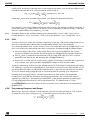
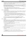
4.1.14 Lock-Unlock Detection
Remembering how the PLL1 works with two current generators (one sink and one source), it
appears that when PLL1 is locked both generators are OFF almost all the time; when out of phase,
one generator will be ON for part of the period. When frequencies differ, one generator or the other
will be ON for approximately half the time (mean value).
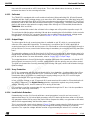
This is used to build a lock-unlock detector (Figure 3) where a gate output is LOW whenever one of
the current sources is ON. It controls very low charge and discharge currents to an internal
capacitor. The capacitor voltage will take a value of approximately 8V when PLL1 is locked, and

Obsolete Product(s) - Obsolete Product(s)
Horizontal Section AN1290
18/62 STMicroelectronics Confidential
approximately 4V when it is unlocked. The last elements are an internal comparator referenced to
6.25V (with hysteresis) and a CMOS inverter; you will find on its output pin 3 a HIGH state when
PLL1 is unlocked. The same data can also be read in the IC through the I²C bus. Nevertheless, a
Read request is necessary in this case.
There may be an ill-defined state and erratic pulses may appear during Lock
↔ Unlock transitions,
mainly when oscillator frequency approaches Lock state. The reasons for this are basic and cannot
be avoided. To prevent malfunctions, provide an external supplementary delay. Since the delay is
external, it can be made longer for the Unlocked
→ Locked transition (thus avoiding the parasitic
pulses), while being kept very short for the opposite Locked
→ Unlocked transition, when
emergency measures should be triggered in a short time.
Because some customers asked for a shorter reaction time to transition Locked
→ Unlocked, the
TDA9112A provides an option through I²C programming (Sad1Fh/d2) for a delay divided by two. Be
aware that as a consequence, a very long composite VSync signal without serration pulses could be
unduly interpreted as a loss of locking.
Further to this indication, as soon as an Unlock state is detected, the oscillator frequency change
rate is decreased. When switching from High to Low frequency, the B+ regulation loop will have
enough time to decrease the B+ value accordingly, thus preventing the destruction of the scanning
transistor by overcurrent and overvoltage. According to the typical application schematic, the
frequency will be reduced by approximately 0.1 kHz/ms.
Since pin 3 is also used for V blanking, levels on pin 3 are defined as follows:
● approximately 0V: locked, not blanked
● higher than 5V: unlocked
● the blanking signal adds to Lock/Unlock level (+1V if Blanked).
The Lock/Unlock signal is available only if selected through I²C programming (Sad16h/d0).
4.1.15 H Moire Cancellation
The Moire phenomenon only takes place on color screens and when displaying grey areas resulting
from an alternation of black and white dots.
It may happen that the succession of black and white dots presents a pitch which is very close to
that of the TV screen. If in an area of the screen, the white dots fall exactly on the tube pixels, then,
at some further distance, they will fall exactly between the pixels. The result will be a succession of
bright and dark stripes with an approximately vertical direction. The nearer the dot pitch to the tube
Figure 3: Lock/Unlock
8V
I
SINK
I
SOURCE
To I²C
6.25V
0V = Lock
1V = Lock, Blank
5V = Unlock
6V = Unlock, Blank
3

Obsolete Product(s) - Obsolete Product(s)
STMicroelectronics Confidential 19/62
AN1290 Horizontal Section
pitch, the wider the stripes (however, if the dot array is not uniform, the basically vertical stripes will
be strongly distorted).
Please notice that if the succession of dots is shifted horizontally by half a pixel, the dark and bright
stripes will be exchanged. This provides a way to compensate the H Moire: by artificially introducing
an horizontal jitter with an amplitude of half a pixel, any point on the screen will be successively on
a dark then bright stripe. As a result the eye will see medium brightness everywhere.
Since Moire can also appear with other less simple combinations of dots and pixels, the setting of
the Moire cancellation must be left to the end user for optimum results.
A self-contained H-Moire cancellation system is available on the TDA9112: an internal logic circuit
provides a series of pulses related to H frequency with an adjustable amplitude through I²C
(Register 02). After a convenient attenuation, this pulsed voltage will modulate the voltage on PLL2
capacitor, introducing the required artificial H jitter. The phase of this jitter is reversed for every other
frame, in order to make it less noticeable.
This Moire cancellation system can be used for any type of monitor (be it common or separate EHV
and H scanning). Two modes can be selected through I²C programming (Sad02h/d7). In the event
of a “common” structure, better results will be obtained when set to 0, while 1 is mandatory with a
“separate” structure. If Moire is not needed, the level must be set to 0 through I²C programming.
On the low-cost TDA9115 version, the Moire compensation is available on pin 11 rather than being
applied internally. First, the pulse amplitude of pin 11 must be divided in a ratio of 1000 to 2000 with
a resistor bridge referenced to HGND. Then connect the low-side end of PLL2 capacitor (formerly
grounded) to the medium point of resistor bridge. This way, the compensation pulses will be applied
to pin 5 through the capacitor.
The TDA9116 provides either internal or external compensation which is selected by I²C
programming (Sad16h/d3:2). When internal compensation is selected, pin 11 becomes a 7-bit DAC
with a span between 0 and 5 V.
4.2 Application Hints
4.2.1 Minimizing Jitter
The TDA9112 provides low intrinsic horizontal jitter, but some care must be taken not to spoil its
naturally good performances. Since all horizontal timings are based on the comparison of the
oscillator sawtooth with various DC levels, all these voltages should be kept perfectly clean. Let us
make a “rule-of-thumb” calculation: if the oscillator sawtooth amplitude: 4.8V, corresponds to 7/8 of
the period, then a 1mV parasitic voltage on either the sawtooth or one of the DC levels will induce:
31778 x (7/8)/4800 = 5.8 ns of jitter in VGA, which is an unacceptable value.
Here are some basic precautions to obtain the best jitter value:
● First, care should be taken not to corrupt the incoming sync pulse. Typically, it will have some
20ns transition time and an 5V amplitude. In these conditions, adding a 0.25 V amplitude
parasitic voltage (ground ripple for instance) will cause 1ns of jitter on the incoming sync.
Similar considerations apply to Hfly pulse, which is not very fast.
More precisely, we can consider that the components of the PLL1 filter have been optimized for
jitter. If jitter is found to decrease when using other values than the ones indicated for theses
components, usually the reason is that the input HSync is already jittered; suppressing this
jitter on the HSync input will lead to a jitter performance unattainable before.
● A separate ground connection, tied to pin 7, should be devoted to all horizontal-related
components, i.e. those connected to pins 4, 5, 6, 8, 9, 10, 12 and 13. This connection must be
tied to pins 21 and 27, but it should not carry any other current, especially those not

Obsolete Product(s) - Obsolete Product(s)
Horizontal Section AN1290
20/62 STMicroelectronics Confidential
synchronized to horizontal components in frequency and phase, like those in SMPS, B+
DC/DC converters, PWM DACs, etc.
— The ground track should enter the IC area through pin 27, then go to the various ground pins
(7, 21, which are not connected internally) and to the H- and V-related components and to
no other place.
● A monitor chassis normally includes several switching circuits, like SMPS, B+ DC/DC
converter.... The high dI/dt value in some wirings of these circuits will induce parasitic voltages
in all neighboring loops. Do not neglect some medium power circuits, like B+ converter gate
drive: even with a low current, the dI/dt value may be high. This will result in a localized jitter
(i.e. only taking place with certain specific settings of the H-position, H-size, brightness, etc.).
● A decoupling capacitor and its connecting tracks constitute a loop where the high dI/dt value
induces voltages. Same for oscillator capacitor Co. These parasitic voltages appear in series
with the capacitor and induce jitter; they will be minimized if the loop (IC pin-capacitor-IC
ground) presents the smallest possible area. The loops that include resistors are less critical.
(Nevertheless, it is advisable to keep the connection to R
0
as short and small as possible to
minimize parasitic capacitance on pin 8).
● The loops emitting parasites obviously should be as small and remote as possible. (SMPS,
DC/DC converter, etc.)
A standard filter for PLL1 (pin 9) includes:
● 10nF to ground;
● in parallel, the series combination of 1.8kΩ and 4.7µF electrolytic.
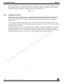
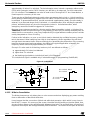
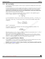
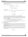
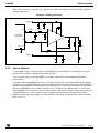
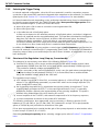
4.2.2 Output Stage
The output stage is a NPN transistor, the collector of which is available on pin 26. It becomes
conductive when the H scanning transistor is to be switched ON. Pin 26 must be tied to the supply
through a pull-up resistor. With a 30mA sink capability, it can control a bipolar driver.
Most often, “reverse” control is used, with a driver stage as shown in Figure 4.
(A MOS driver is shown. For an application with a bipolar driver, refer to Evaluation Board booklet).
The following points have to be considered:
Figure 4: Driver Stage with MOSFET
H scanning
transistor
Transformer
supply
Driver supply
IC supply
26
27
La pagina sta caricando ...
La pagina sta caricando ...
La pagina sta caricando ...
La pagina sta caricando ...
La pagina sta caricando ...
La pagina sta caricando ...
La pagina sta caricando ...
La pagina sta caricando ...
La pagina sta caricando ...
La pagina sta caricando ...
La pagina sta caricando ...
La pagina sta caricando ...
La pagina sta caricando ...
La pagina sta caricando ...
La pagina sta caricando ...
La pagina sta caricando ...
La pagina sta caricando ...
La pagina sta caricando ...
La pagina sta caricando ...
La pagina sta caricando ...
La pagina sta caricando ...
La pagina sta caricando ...
La pagina sta caricando ...
La pagina sta caricando ...
La pagina sta caricando ...
La pagina sta caricando ...
La pagina sta caricando ...
La pagina sta caricando ...
La pagina sta caricando ...
La pagina sta caricando ...
La pagina sta caricando ...
La pagina sta caricando ...
La pagina sta caricando ...
La pagina sta caricando ...
La pagina sta caricando ...
La pagina sta caricando ...
La pagina sta caricando ...
La pagina sta caricando ...
La pagina sta caricando ...
La pagina sta caricando ...
La pagina sta caricando ...
La pagina sta caricando ...
-
 1
1
-
 2
2
-
 3
3
-
 4
4
-
 5
5
-
 6
6
-
 7
7
-
 8
8
-
 9
9
-
 10
10
-
 11
11
-
 12
12
-
 13
13
-
 14
14
-
 15
15
-
 16
16
-
 17
17
-
 18
18
-
 19
19
-
 20
20
-
 21
21
-
 22
22
-
 23
23
-
 24
24
-
 25
25
-
 26
26
-
 27
27
-
 28
28
-
 29
29
-
 30
30
-
 31
31
-
 32
32
-
 33
33
-
 34
34
-
 35
35
-
 36
36
-
 37
37
-
 38
38
-
 39
39
-
 40
40
-
 41
41
-
 42
42
-
 43
43
-
 44
44
-
 45
45
-
 46
46
-
 47
47
-
 48
48
-
 49
49
-
 50
50
-
 51
51
-
 52
52
-
 53
53
-
 54
54
-
 55
55
-
 56
56
-
 57
57
-
 58
58
-
 59
59
-
 60
60
-
 61
61
-
 62
62


ST TDA9113 Application Note
- Tipo
- Application Note
- Questo manuale è adatto anche per
in altre lingue
- English: ST TDA9113
Altri documenti
-
Pioneer PR-8210-A Manuale utente
-
Behringer ABACUS Guida Rapida
-
HP 1123A Manuale utente
-
Realistic MG-1 Manuale utente
-
Zenith PRO1200X Guida d'installazione
-
Eurotherm 306 6 channel multi point recorder Manuale del proprietario
-
-
Philips 107P50/97 Manuale utente
-
Philips 109B50/97 Manuale utente
-