MATSONIC MS7132A Manuale utente
- Categoria
- Schede madri
- Tipo
- Manuale utente

TRADEMARK
All products and company names are trademarks or registered
trademarks of their respective holders.
These specifications are subject to change without notice.
Manual Revision 6.0
October 12, 1999
MS7132AMS7132A
MS7132AMS7132A
MS7132A
A PA P
A PA P
A P
entiumentium
entiumentium
entium
®®
®®
®
II or P II or P
II or P II or P
II or P
entiumentium
entiumentium
entium
®®
®®
®
III III
III III
III
Slot1 Processor based AGPSlot1 Processor based AGP
Slot1 Processor based AGPSlot1 Processor based AGP
Slot1 Processor based AGP
mainboarmainboar
mainboarmainboar
mainboar
d (100/66MHz)d (100/66MHz)
d (100/66MHz)d (100/66MHz)
d (100/66MHz)
SupporSuppor
SupporSuppor
Suppor
ts PC-133 SDRAM Modulets PC-133 SDRAM Module
ts PC-133 SDRAM Modulets PC-133 SDRAM Module
ts PC-133 SDRAM Module

MS7132A
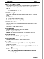
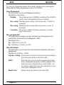
Table of Contents
Section 1 Introduction
Components Checklist ....................................... 1-1
Overview
Pentium
®
II or Pentium
®
III Processor ............... 1-2
S.E.C. Cartridge Terminology ........................... 1-3
Accelerated Graphics Port ................................ 1-4
Hardware Monitoring........................................ 1-4
MS7132A Form-factor ...................................... 1-5
I/O Shield Connector......................................... 1-6
Power-On/Off (Remote).................................... 1-6
System Block Diagram ...................................... 1-7
Section 2 Features
MS7132A Features............................................ 2-1
Section 3 Installation
MS7132A Detailed Layout................................ 3-1
Easy Installation Procedure
Configure DIP Switch........................................ 3-3
System Memory Configuration .......................... 3-4
Installing a Pentium
®
II Processor ..................... 3-7
Device Connectors ............................................ 3-9
External Modem Ring-in Power On and
Keyboard Power On Function (KBPO) ............. 3-11
Section 4 Award BIOS Setup
BIOS Instructions .............................................. 4-1
Standard CMOS Setup....................................... 4-2
BIOS Features Setup ......................................... 4-3
Chipset Features Setup ...................................... 4-8

MS7132A
Power Management Setup ................................. 4-11
PNP/PCI Configuration ..................................... 4-15
Load Setup Defaults .......................................... 4-17
Integrated Peripherals........................................ 4-17
Sensor and CPU Speed Setup ............................ 4-22
Change Supervisor or User Password ............... 4-24
IDE HDD Auto Detection.................................. 4-25
Save & Exit Setup ............................................. 4-27
Exit Without Saving ........................................... 4-27
Section 5 Appendix
Appendix A
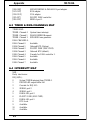
Memory Map ..................................................... A-1
I/O Map ............................................................. A-1
Timer & DMA Channels Map ........................... A-2
Interrupt Map..................................................... A-2
RTC & CMOS RAM Map ................................. A-3
Appendix B
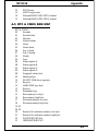
POST Codes...................................................... A-5
Unexpected Errors............................................. A-8
Appendix C
Load Setup Defaults .......................................... A-9
Appendix D
GHOST 5.1 Quick User’s Guide ....................... A-11

MS7132A
Page Left Blank

Introduction
MS7132A
Page 1-1
Section 1
INTRODUCTION
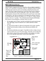
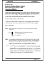
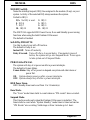
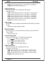
Components Checklist
üü
üü
ü A. (1) MS7132A mainboard
üü
üü
ü B. (1) MS7132A user’s manual
üü
üü
ü C. (1) Floppy ribbon cable
üü
üü
ü D. (1) ATA-66 Hard drive ribbon cable
üü
üü
ü E. (1) Foldable Retention Module
F. (1) Heatsink Support Unit (Optional)
G. (1) PS/2 to AT keyboard connector adapter (optional)
üü
üü
ü H. (1) Driver and utility
A
E
G
B
USER’S
MANUAL
MS7132A
F
Top Half
Bottom Half
H
or
D
C

Introduction
MS7132A
Page 1-2
Overview
Pentium
®
II or Pentium
®
III Processor
The Pentium
®
II or Pentium
®
III Processor is the follow-on to the Pentium
®
Processor. The Pentium
®
II or Pentium
®
III Processor, like the Pentium
®
Pro
processor, implements a Dynamic Execution micro-architecture -- a unique
combination of multiple branch prediction, data flow analysis, and speculative
execution. This enables the Pentium
®
II Processor to deliver higher performance
than the Pentium
®
processor, while maintaining binary compatibility with all
previous Intel architecture processors.
A significant feature of the Pentium
®
II or Pentium
®
III Processor, from a system
perspective, is the built-in direct multiprocessing support. In order to achieve
multiprocessing, and maintain the memory and I/O bandwidth to support it, new
system designs are needed. For systems with dual processors, it is important to
consider the additional power burdens and signal integrity issues of supporting
multiple loads on a high speed bus. The Pentium
®
II or Pentium
®
III Processor
can supports both uni-processor and dual processor implementations.
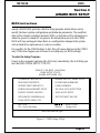
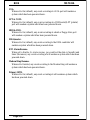
The Pentium
®
II or Pentium
®
III Processor utilizes Single Edge Contact (S.E.C.)
(Figure 1) cartridge packaging technology. The S.E.C. cartridge allows the L2
cache to remain tightly coupled to the processor, while maintaining flexibility when
implementing high performance processors into OEM systems. The second level
cache is performance optimized and tested at the cartridge level. The S.E.C.
cartridge utilizes surface mounted core components and a printed circuit board
with an edge finger connection. The S.E.C. cartridge package introduced on the
Pentium
®
II Processor will also be used in future Slot 1 processors.
The S.E.C. cartridge has the following features: a thermal plate, a cover and a
PCB with an edge finger connection. The thermal plate allows standardized
heatsink attachment or customized thermal solutions. The thermal plate enables a
reusable heatsink to minimize fit issues for serviceability, upgradeability and
replacement. The full enclosure also protects the surface mount components.
The edge finger connection maintains socketabilty for system configuration. The
edge finger connector is denoted as ‘Slot 1 connector’ in this and other
documentation.

Introduction
MS7132A
Page 1-3
The entire enclosed product is called the Pentium
®
II or Pentium
®
III Processor.
The packaging technology and each of the physical elements of the product are
referred to using accurate technical descriptions. This allows clear reference to
the products as just a processor. This is the model used in past packaging tech-
nologies like PGA, TCP, PQFP, DIP, etc.
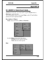
S.E.C. Cartridge Terminology
• Pentium
®
II or Pentium
®
III Processor
The new enclosed card packaging technology is called a “Single Edge
Contact cartridge.” This is similar to previous names for packaging
technology such as PGA or TCP.
• Processor card
The green PCB (with or without components on it)
• Processor core
The silicon on the PLGA package on the PCB
• Cover
The plastic cover on the opposite side from the thermal plate.
• Slot 1
The slot that the S.E.C. cartridge plugs into, just as the Pentium
®
Pro
processor uses Socket 8.
• Retention mechanism
Formerly ‘retention module’ the dual posts, etc. that holds the cartridge in
place.
• Thermal plate
The heatsink attach-
ment plate.
• Heat sink supports
The support pieces that
are mounted on the
mainboard to provide
added support for
heatsinks.
Figure 1: Pentium
®
II/III Processor CPU
with S.E.C.C. or S.E.C.C.2 Package
Pentium
®
II Processor
in an S.E.C.C. Package
Pentium
®
III Processor
in an S.E.C.C.2 Package

Introduction
MS7132A
Page 1-4
The L2 cache (TagRAM, PBSRAM) components keep standard industry names.
The Pentium
®
II or Pentium
®
III Processor is the first product to utilize the S.E.C.
cartridge technology and Slot 1 connector. Unless otherwise noted, any references
to “Pentium
®
II Processor”, “Pentium
®
II or Pentium
®
III Processor/Slot 1 proces-
sor” or “Pentium
®
III Processor” will apply to both the Pentium
®
II Processor
desktop processors.
Accelerated Graphics Port
(AGP or A.G.P.)
Typically, 3D graphics rendering requires a tremendous amount of memory, and
demands ever increasing throughput speed as well. As 3D products for the
personal computer become more and more popular, these demands will only
increase. This will cause a rise in costs for both end users and manufacturers.
Lowering these costs as well as improving performance is the primary motivation
behind AGP. By providing a massive increase in the bandwidth available between
the video card and the processor, it will assist in relieving some of these pressures
for quite sometime.
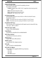
Hardware Monitoring
Hardware monitoring allows you to monitor various aspects of your systems
operations and status. The features include CPU temperature, voltage and RPM
of fan.

Introduction
MS7132A
Page 1-5
MS7132A Form-Factor
The MS7132A is designed with ATX form factor - the new industry standard of
chassis. ATX form factor is essentially a Baby-AT baseboard rotated 90 degrees
within the chassis enclosure and a new mounting configuration for the power
supply. With these changes the processor is relocated away from the expansion
slots, allowing them all to hold full length add-in cards. ATX defines a double
height aperture to the rear of the chassis which can be used to host a wide range
of onboard I/O. Only the size and position of this aperture is defined, allowing
PC manufacturers to add new I/O features (e.g.; TV input, TV output, joystick,
modem, LAN, etc.) to systems. This will help systems integrators differentiate
their products in the marketplace, and better meet your needs.
• By integrating more I/O down onto the board and better positioning the hard
drive and floppy connectors material cost of cables and add-in cards is
reduced.
• By reducing the number of cables and components in the system, manufac-
turing time and inventory holding costs are reduced and reliability will
increase.
• By using an optimized power supply, it's possible to reduce cooling costs and
lower acoustical noise. An ATX power supply, which has a side-mounted fan,
allows direct cooling of the processor and add-in cards making a secondary
fan or active heatsink unnecessary in most system applications.
Full length
slots
Expandable I/O
5 1/4"
Bay
3 1/2"
Bay
Figure 2: Summary of ATX chassis features
CPU located near
Power Supply
Single chassis
fan for
system
ATX
Power
Supply
ATX power
connector
Floppy / IDE
connectors
close to
peripheral
bays

Introduction
MS7132A
Page 1-6
MS7132A Board
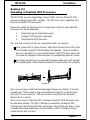
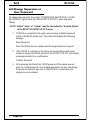
Power-On/Off (Remote)
The MS7132A has a single 20-pin connector for ATX power supplies. For ATX
power supplies that support the Remote On/Off feature, this should be connected
to the systems front panel for system Power On/Off button. The systems power
On/Off button should be a momentary button that is normally open.
The MS7132A has been designed with “Soft Off" functions. You can turn Off the
system from one of two sources: The first is the front panel Power On/Off
button, and the other is the "Soft Off" function (coming from the MS7132A’s
onboard circuit controller) that can be controlled by the operating system. Win-
dows 95/98 will control this when the user clicks that they are ready to Shutdown
the system.
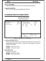
Figure 4: Simple ATX Power ON/OFF Controller
J 3
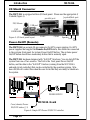
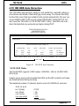
I/O Shield Connector
The MS7132A is equipped with an I/O back panel. Please use the appropriate I/
O shield (figure 3).
PS/2 Mouse
PS/2
KEYBOARD
USB port
COM1 COM2
parallel port
Speaker
Line_in
MIC
Figure 3: I/O back panel layout
Joystick/Midi port
ATX
POWER SUPPLY
Case (chassis) Power
ON/OFF button (J 3)

Introduction
MS7132A
Page 1-7
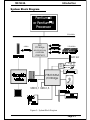
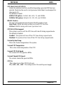
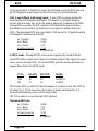
Figure 5: System Block Diagram
System Block Diagram
PAC
PCI Bridge
and memory
controller
VT82C693
100/66MHz
100/66MHz
66MHz
Pentium II
or
Processor
Pentium III
VT82C686A
I/O Bridge
AC
97
USB 0,1 USB 2,3
AMR Slot

Introduction
MS7132A
Page 1-8
Page Left Blank

Features
MS7132A
Page 2-1
Section 2
FEATURES
MS7132A Features:
• MS7132A is based on the Pentium
®
II/III Processor operating at 266 ~
550MHz on Slot1. The board is configured by an ESSJ (Easy-Setting-
Single-Jumper) to match your CPU clock speed.
• Designed with VIA Apollo Pro+ PCIset.
• Supports up to 768MB of DRAM (minimum of 8 MB) on board (please
see Section 3-2).
• MS7132A will support Error Checking and Correcting (ECC) when using
parity SDRAM memory modules. This will detect multiple bit errors and
correct 1-bit memory errors.
• Supports (1) 16 bit ISA slots, (5) 32 bit PCI slots, (1) AGP slot, (1) AMR
slot and provides (2) independent high performance PCI IDE interfaces
capable of supporting PIO Mode 3/4 and Ultra DMA 33/66 devices.
The MS7132A supports (5) PCI Bus Master slots and a jumperless PCI
INT# control scheme which reduces configuration confusion when plugging
in PCI card(s).
• Supports ATAPI (e.g. CD-ROM) devices on both Primary and Secondary
IDE interfaces.
• Designed with on chip Multi I/O: (1) floppy port, (1) parallel port (EPP,
ECP), and (2) serial ports (16550 Fast UART).
Note: Japanese “Floppy 3 mode” is also supported
• Features Award Plug & Play BIOS. With Flash Memory you can always
upgrade to the current BIOS as they are released.
• MS7132A utilizes a Lithium battery which provides environmental protec
tion and longer battery life.
• Supports the (4) Universal Serial Bus (USB) Ports. The onboard
VT82C686A chip provides the means for connecting PC peripherals such
as; keyboards, joysticks, telephones, and modems.

Features
MS7132A
Page 2-2
• Built-in ATX 20-pin power supply connector.
• Software power-down when using Windows
®
95/98.
• Supports ring-in feature (remote power-on through external modem,
allows system to be turned on remotely).
• Resume by Alarm - Allows your system to turn on at a preselected time.
• Power Loss Recovery - In the event of a power outtage your system will
automatically turn itself back on without user intervention.
• Supports CPU Hardware sleep and SMM (System Management Mode).
• Supports Keyboard power ON function (KBPO).
• Built-in WOL (Wake-up On Lan) Connector.
• Built-in AC97 PCI Audio.

Installation
MS7132A
Page 3-1
Section 3
INSTALLATION

Installation
MS7132A
Page 3-2
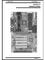
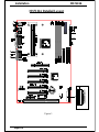
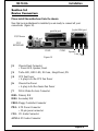
Figure 1
MS7132A Detailed Layout

Installation
MS7132A
Page 3-3
Easy Installation Procedure
Easy Installation Procedure
The following must be completed before powering on your new system:
3-1. Configure DIP Switch and Jumper to match your hardware
3-2. System memory Configuration
3-3. Install Pentium II or Pentium III Processor
3-4. Device Connectors
3-5 External Modem Ring-in Power ON and Keyboard Power ON
Functions (KBPO)
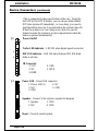
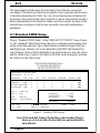
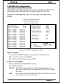
Section 3-1
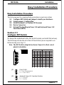
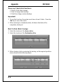
Configure DIP Switch
We design this motherboard with a DIP Switch to make your install fast and easy.
The following will describe all of the DIP Switch that you are required to set
before moving on to step 3-2.
Note: The DIP Switch as depicted as shown (Figure 1) in their correct
physical orientation.
JP1 Clear COMS
1-2 : Run Mode(default)
2-3 : Clear CMOS
JP4 Keyboard Power-ON Function Selection
1-2 : Disabled
2-3 : Enabled
1
2
34
ON
1WS)zHM(UPC
1234 oitaRzHM66zHM001
NONONOX3002003
NONOX5.3332053
NONONOX4662004
NONOX5.4003054
NONOX5333005
NOX5.5663055*
NONONOX6004006*
NONOX5.6334056*
NONOX7664*007*
NOX5.7005*057*
NONOX8335*008*
*reserved

Installation
MS7132A
Page 3-4
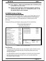
Section 3-2
System Memory Configuration
Memory Layout
The MS7132A supports (3) PC133 168-pin DIMMs (Dual In-line Memory
Module). The DIMMs can be either EDO (Enhanced Data Out) or SDRAM
(Synchronized DRAM).
• DIMM SDRAM may be 83MHz (12ns), 100MHz (10ns) or
125MHz (8ns) bus speed.
• If you use both 50ns and 60ns memory you must configure
your BIOS to read 60ns.
• When using Synchronous DRAM we recommend using the
4 clock variety over the 2 clock.
Figure 2 and Table 1 show several possible memory configurations using both
SIMM and DIMM.
* SDRAM only supports 8, 16, 32, 64, 128, 256MB DIMM modules.
* We recommend to use PC100 Memory Module for bus speed between 66MHz
and 100MHz and PC133 Memory for bus speed over 100MHz.
* Using non-compliant memory with higher bus speed (over clocking) may
severely compromise the integrity of the system.
DIMM 1
DIMM 2
Bank 0/1
Bank 2/3
DIMM 3
Bank 4/5
-Synchronous
-EDO
yromeMlatoT
1MMID
)1/0knaB(
2MMID
)3/2knaB(
3MMID
)5/4knaB(
BM652=
mumixaM
*MARDS/ODE
,BM46,BM23,BM61,BM8
1XBM652,BM821
enoNenoN
BM215=
mumixaM
*MARDS/ODE
,BM46,BM23,BM61,BM8
1XBM652,BM821
*MARDS/ODE
,BM46,BM23,BM61,BM8
1XBM652,BM821
enoN
BM867=
mumixaM
*MARDS/ODE
,BM46,BM23,BM61,BM8
1XBM652,BM821
*MARDS/ODE
,BM46,BM23,BM61,BM8
1XBM652,BM821
*MARDS/ODE
,BM46,BM23,BM61,BM8
1XBM652,BM821
Figure 2
Table 1

Installation
MS7132A
Page 3-5
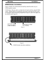
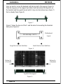
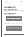
DIMM Module Installation
Figure 3 displays the notch marks and what they should look like on your
DIMM memory module.
DIMMs have 168-pins and two notches that will match with the onboard DIMM
socket. DIMM modules are installed by placing the chip firmly into the socket
at a 90 degree angle and pressing straight down (figure 4) until it fits tightly into
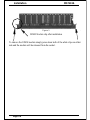
the DIMM socket (figure 5).
Figure 3
Figure 4
DIMM Module clip before installation
LEFT KEY ZONE
(UNBUFFERED)
CENTER KEY ZONE
(3.3 V DRAM)

Installation
MS7132A
Page 3-6
Figure 5
DIMM Module clip after installation
To remove the DIMM module simply press down both of the white clips on either
side and the module will be released from the socket.
La pagina sta caricando ...
La pagina sta caricando ...
La pagina sta caricando ...
La pagina sta caricando ...
La pagina sta caricando ...
La pagina sta caricando ...
La pagina sta caricando ...
La pagina sta caricando ...
La pagina sta caricando ...
La pagina sta caricando ...
La pagina sta caricando ...
La pagina sta caricando ...
La pagina sta caricando ...
La pagina sta caricando ...
La pagina sta caricando ...
La pagina sta caricando ...
La pagina sta caricando ...
La pagina sta caricando ...
La pagina sta caricando ...
La pagina sta caricando ...
La pagina sta caricando ...
La pagina sta caricando ...
La pagina sta caricando ...
La pagina sta caricando ...
La pagina sta caricando ...
La pagina sta caricando ...
La pagina sta caricando ...
La pagina sta caricando ...
La pagina sta caricando ...
La pagina sta caricando ...
La pagina sta caricando ...
La pagina sta caricando ...
La pagina sta caricando ...
La pagina sta caricando ...
La pagina sta caricando ...
La pagina sta caricando ...
La pagina sta caricando ...
La pagina sta caricando ...
La pagina sta caricando ...
La pagina sta caricando ...
La pagina sta caricando ...
La pagina sta caricando ...
La pagina sta caricando ...
La pagina sta caricando ...
La pagina sta caricando ...
La pagina sta caricando ...
La pagina sta caricando ...
La pagina sta caricando ...
La pagina sta caricando ...
La pagina sta caricando ...
La pagina sta caricando ...
La pagina sta caricando ...
La pagina sta caricando ...
-
 1
1
-
 2
2
-
 3
3
-
 4
4
-
 5
5
-
 6
6
-
 7
7
-
 8
8
-
 9
9
-
 10
10
-
 11
11
-
 12
12
-
 13
13
-
 14
14
-
 15
15
-
 16
16
-
 17
17
-
 18
18
-
 19
19
-
 20
20
-
 21
21
-
 22
22
-
 23
23
-
 24
24
-
 25
25
-
 26
26
-
 27
27
-
 28
28
-
 29
29
-
 30
30
-
 31
31
-
 32
32
-
 33
33
-
 34
34
-
 35
35
-
 36
36
-
 37
37
-
 38
38
-
 39
39
-
 40
40
-
 41
41
-
 42
42
-
 43
43
-
 44
44
-
 45
45
-
 46
46
-
 47
47
-
 48
48
-
 49
49
-
 50
50
-
 51
51
-
 52
52
-
 53
53
-
 54
54
-
 55
55
-
 56
56
-
 57
57
-
 58
58
-
 59
59
-
 60
60
-
 61
61
-
 62
62
-
 63
63
-
 64
64
-
 65
65
-
 66
66
-
 67
67
-
 68
68
-
 69
69
-
 70
70
-
 71
71
-
 72
72
-
 73
73


MATSONIC MS7132A Manuale utente
- Categoria
- Schede madri
- Tipo
- Manuale utente
in altre lingue
- English: MATSONIC MS7132A User manual
